


Bridging the Frontier Bob Smith, Executive Director
Bob Smith is Executive Director of the ESD Alliance responsible for its management and operations. Previously, Bob was senior vice president of Marketing and Business Development at Uniquify, responsible for brand development, positioning, strategy and business development activities. Bob began his … More » Ansys’ John Lee on Cultivating Trust within his TeamMay 9th, 2024 by Bob Smith, Executive Director
 Note: Bob Smith’s interview below with John Lee of Ansys originally appeared March 4, 2024 on the SEMI website blog. Cultivating trust and keeping his team agile and innovative as they engage with technology partners and customers is a core focus of John Lee, General Manager and Vice President of the Ansys Electronics, Semiconductors, and Optics Business Unit. I recently spoke with Lee, a serial entrepreneur and a member of the ESD Alliance Governing Council, about his career and move from technical roles into management and how he motivates members of his team. Read the rest of Ansys’ John Lee on Cultivating Trust within his Team CEO Executive Outlook Last Call, Spotlight on ESD Alliance VolunteersMay 2nd, 2024 by Paul Cohen
 Scott Seiden Kudos to Scott Sieden, Keysight’s Director Strategic Marketing, Keysight EDA Portfolio, and a tireless ESD Alliance volunteer, for his efforts to ensure a lively CEO Executive Outlook next Thursday, May 9. A highlight of the evening are two RISC-V influencers who will discuss the RISC-V movement and its effect on the semiconductor design ecosystem –– Calista Redmond, CEO of RISC-V International, and Jack Kang, Senior Vice President of Business Development at SiFive. Bob Smith, the ESD Alliance’s Executive Director, will moderate a panel of executives reviewing the state of the electronic system design industry now and in the future:
Read the rest of CEO Executive Outlook Last Call, Spotlight on ESD Alliance Volunteers Curvy Design’s Time Has Come Says D2S CEO Aki FujimuraApril 23rd, 2024 by Bob Smith, Executive Director
Aki Fujimura, CEO of D2S and a member of the ESD Alliance Governing Council, is an expert on curvilinear (aka curvy) chip design. He believes curvy chip design’s time has come and will ultimately replace the traditional Manhattan routing methods with their 90-degree-constrained turns. He recently discussed with me why curvy designs will lead to smaller, faster and more power efficient devices. Smith: As the original creator of DEF/LEF as VP Engineering of Tangent in the late 1980s, you are very familiar with Manhattan routing methods. Tangent was first to commercialize area-based placement and routing with DEF, LEF, engineering change order (ECO), clock tree synthesis, scan insertion, timing-driven design in a then-solidifying synchronous design methodology. Tangent was acquired by Cadence in 1989 as a result. DEF/LEF are still the standard formats today for place and route. Isn’t the whole EDA infrastructure still pretty much making the Manhattan assumption? Fujimura: A huge amount of innovation since then has improved considerably upon what we did back then. But you’re right that the basic approach to place and route is still making the Manhattan assumption with an alternating preferred direction (either horizontal or vertical) per layer. The Manhattan assumption was already there before Tangent came along. But prior to DEF/LEF, all interconnect was described as a path with (x,y) of each vertex. DEF/LEF halved the file sizes through the simple assumption that X or Y repeat because 99% of wires are alternatingly horizontal and vertical. Read the rest of Curvy Design’s Time Has Come Says D2S CEO Aki Fujimura Great Lineup of Speakers Highlights CEO Executive Outlook May 9 at KeysightApril 17th, 2024 by Bob Smith, Executive Director
Registration may still be open for the ESD Alliance CEO Executive Outlook co-hosted with Keysight Technologies Thursday, May 9, but I suggest you sign up now. With a great lineup of speakers and topical discussions, we’re expecting a crowd. We have a slight change in speakers. Jack Kang, Senior Vice President of Sales and Business Development at SiFive, joins Calista Redmond, CEO of RISC-V International, to talk about the evolving RISC-V movement and its effect on the semiconductor design ecosystem. Read the rest of Great Lineup of Speakers Highlights CEO Executive Outlook May 9 at Keysight Electronic System Design Industry Logs $4.4 Billion in Revenue in Q4 2023April 9th, 2024 by Paul Cohen
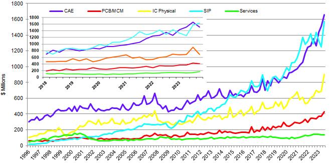
Kudos all around our industry as it continues to report strong revenue growth! According to the Electronic Design Market Data (EDMD) report, the Electronic System Design (ESD) industry revenue increased 14% to $4,423 million in the fourth quarter of 2023 from the $3,879.9 million logged in the third quarter of 2023. The four-quarter moving average comparing the most recent four quarters to the prior four increased 14.1%.
Our industry’s hiring. Companies tracked employed 60,106 people globally in Q4 2023, an 8.9% jump over the Q4 2022 headcount of 55,192 and up 0.6% compared to Q3 2023. Read the rest of Electronic System Design Industry Logs $4.4 Billion in Revenue in Q4 2023 Keysight to Co-Host ESD Alliance 2024 CEO Executive Outlook Featuring RISC-V ExecutivesMarch 28th, 2024 by Bob Smith, Executive Director
Registration is now open for our annual CEO Executive Outlook co-hosted with Keysight Technologies that will be held Thursday, May 9, in Santa Clara, Calif. The formal program will begin with two high-profile executives –– Calista Redmond, CEO of RISC-V International, and Patrick Little, CEO of SiFive, a RISC-V IP provider. They will address the evolving RISC-V movement and its effect on the semiconductor design ecosystem. Immediately following their talk will be a panel of noteworthy executives who will discuss the state of the electronic system design industry and the outlook for the future. I will moderate the panel that features:
The in-person event will be held at Keysight (address below) beginning at 5:30 p.m. P.D.T with networking, dinner and beverages. The program starts at 6:45 p.m. and is open to ESD Alliance and SEMI members at a cost of $25. Pricing for non-members is $50 per person. Click here to register. Keysight 5301 Stevens Creek Blvd., Building 5 Santa Clara About the ESD Alliance For EDACafe readers unfamiliar with the ESD Alliance, a SEMI Technology Community, we represent members of the ecosystem that provides goods and services spanning the conceptualization, design, verification, manufacturing and deployment of semiconductor-based electronic systems. Our industry is essential to the global semiconductor industry as the driving force that enables new electronic systems to be conceived, designed and brought to market. We focus on initiatives and activities that bring value to our entire industry:
Contact me at bsmith@semi.org or Paul Cohen at pcohen@semi.org if you have questions or would like information about joining us. Engage with the ESD Alliance ESD Alliance Bridging the Frontier blog Twitter: @ESDAlliance How One Company Tackled Unlicensed Use of its SoftwareMarch 19th, 2024 by Bob Smith, Executive Director
Note: The ESD Alliance, a SEMI Technology Community, spearheaded an industry joint development effort to develop a server certification protocol to close a loophole often exploited in software piracy schemes. Cadence Design Systems, Siemens EDA and Synopsys were members of the industry-standard SEMI Server Certification Protocol (SSCP) joint development committee. One of many SSCP supporters is Ted Miracco, a founder and executive vice president of AWR Corporation, now part of Cadence, and someone at the forefront of combatting software piracy. My blog post below, originally appearing on Semiconductor Engineering, is based on an interview I did recently with Ted. Piracy is a growing concern for all software providers, especially those of us with complex and specialized software, such as chip design automation software that is expensive to develop and maintain. That’s why the Electronic System Design Alliance (ESD Alliance), a SEMI Technology Community, spearheaded an industry joint development effort to develop a server certification protocol that would close a loophole often exploited in software piracy schemes. Cadence Design Systems, Siemens EDA and Synopsys were members of the industry-standard SEMI Server Certification Protocol (SSCP) joint development committee. SSCP is applicable to protecting any high-value software product(s) that use license management systems to control access to and use of software licenses. It is now available for licensing from SEMI. Read the rest of How One Company Tackled Unlicensed Use of its Software Now Open: Nominations for Phil Kaufman Award and Hall of FameMarch 5th, 2024 by Paul Cohen
Nominations are being accepted now through June 30 for the 2024 Phil Kaufman Award and the Phil Kaufman Hall of Fame, sponsored by the ESD Alliance, a SEMI Technology Community, and the IEEE Council on Electronic Design Automation (CEDA). Nomination forms are available for download on the SEMI website. The awards recognize individuals whose contributions made an impact within electronic system design in business, industry direction, promotion, technology and engineering, educational or mentoring. Established in 1994, the Phil Kaufman Award honors electronic design automation industry pioneer Phil Kaufman, who turned innovative technologies such as silicon compilation and emulation into businesses that have benefited electronic designers. Last year’s recipient was Dr. Lawrence T. Pileggi, Coraluppi Head and Tanoto Professor of Electrical and Computer Engineering at Carnegie Mellon University. The Phil Kaufman Hall of Fame posthumously recognizes individuals who made significant and noteworthy contributions through creativity, entrepreneurism and innovation to the electronic system design industry and were not recipients of the Phil Kaufman Award. Read the rest of Now Open: Nominations for Phil Kaufman Award and Hall of Fame Tackling Cyber Threats and Ensuring Hardware Integrity with Secure Chip Design FlowFebruary 27th, 2024 by Bob Smith, Executive Director
 Note: The blog post below originally appeared on SEMI. Protecting advanced computing infrastructure and the electronic devices that underpin our global economies, businesses and personal lives is essential in the face of growing cybersecurity threats. Cybersecurity protections have traditionally been focused on safeguarding software running on an existing electronic system that can be exploited by malware, trojans, or other malicious code. These threats can be hidden deep within an application, operating system, or BIOS. However, we can no longer give short shrift to the possibility that security threats can infiltrate chip design. Malicious logic can lurk in the design, waiting to be triggered after the chip is manufactured and inside an electronic system. Recent headlines point to the vulnerability of hardware and how cyber threats now target the very building blocks of our digital infrastructure [1,2,3,4]. Hardware design threats can be introduced at various stages of the design flow including specification, architecture, RTL, gate, circuit, or layout. Addressing these threats during semiconductor design will require the industry to acknowledge the issues and re-think how designs are conceptualized and developed so that vulnerabilities can be mitigated as early as possible. Curvy Design’s Time Has Come, Believes D2S CEO Aki FujimuraFebruary 22nd, 2024 by Bob Smith, Executive Director
 Note: The Q&A below first appeared on SEMI in early February. Aki Fujimura, CEO of D2S and a member of the ESD Alliance Governing Council, is an expert on curvilinear (aka curvy) chip design. He believes curvy chip design’s time has come and will ultimately replace the traditional Manhattan routing methods with their 90-degree-constrained turns. He recently discussed with me why curvy designs will lead to smaller, faster and more power efficient devices. Smith: As the original creator of DEF/LEF as VP Engineering of Tangent in the late 1980s, you are very familiar with Manhattan routing methods. Tangent was first to commercialize area-based placement and routing with DEF, LEF, engineering change order (ECO), clock tree synthesis, scan insertion, timing-driven design in a then-solidifying synchronous design methodology. Tangent was acquired by Cadence in 1989 as a result. DEF/LEF are still the standard formats today for place and route. Isn’t the whole EDA infrastructure still pretty much making the Manhattan assumption? Fujimura: A huge amount of innovation since then has improved considerably upon what we did back then. But you’re right that the basic approach to place and route is still making the Manhattan assumption with an alternating preferred direction (either horizontal or vertical) per layer. The Manhattan assumption was already there before Tangent came along. But prior to DEF/LEF, all interconnect was described as a path with (x,y) of each vertex. DEF/LEF halved the file sizes through the simple assumption that X or Y repeat because 99% of wires are alternatingly horizontal and vertical. Read the rest of Curvy Design’s Time Has Come, Believes D2S CEO Aki Fujimura |
|
|
|||||
|
|
|||||
|
|||||


 Animation, 3D Art and 3D Models")