NHanced Semiconductors

The USA’s First Pure-Play Advanced Packaging Foundry

NHanced Semiconductors

The USA’s First Pure-Play Advanced Packaging Foundry.

Foundry 2.0 is Here

At NHanced Semiconductors we transform bleeding-edge designs into state-of-the-art 3DICs and 2.5D assemblies. By integrating dies and chiplets from traditional foundries into new and sophisticated combinations, we offer uniquely customized system-level solutions, merging best-of-class components regardless of source, scale, or material. This new manufacturing model empowers breakthrough innovations. We call it Foundry 2.0™.
https://nhanced-semi.com/wp-content/uploads/2024/02/Home-Foundry.png

Foundry 2.0 is Here

At NHanced Semiconductors we transform bleeding-edge designs into state-of-the-art 3D ICs and 2.5D assemblies. By integrating dies and chiplets from traditional foundries into new and sophisticated combinations, we offer uniquely customized system-level solutions, merging best-of-class components regardless of source, scale, or material. This new manufacturing model empowers breakthrough innovations. We call it Foundry 2.0.
https://nhanced-semi.com/wp-content/uploads/2024/02/Home-Foundry.png
https://nhanced-semi.com/wp-content/uploads/2024/02/Home-Services.png

SERVICESIsn’t It Time to NHance Your Device?

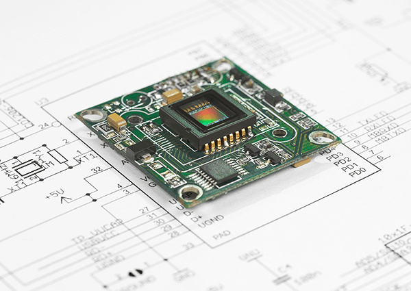
Customers bring us their ideas for advanced devices and specialized sensors. We carry these ideas from start to finish, serving as a complete supply chain partner.

We collaborate, customize, and control the process — from multi-die design and prototyping to sourcing, advanced packaging, package assembly, and final test.

MARKETSPurpose-Built for Specialty Markets

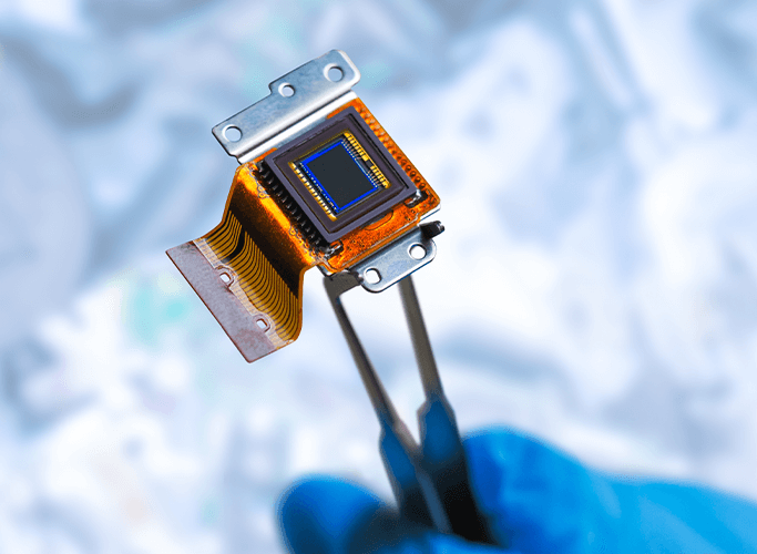
We focus on serving the needs of smaller market segments by performing cost-effective high-mix manufacturing at low and medium volumes.

Whether the project is industrial, medical, military, or scientific, we deliver system-level solutions for specialized and unique devices and sensors.

https://nhanced-semi.com/wp-content/uploads/2024/02/Markets.png
https://nhanced-semi.com/wp-content/uploads/2024/02/Technologies.png

TECHNOLOGIESBrilliant Concepts Deserve Brilliant Implementation

Many of today’s leading-edge products would benefit by 3D or 2.5D architecture using advanced packaging. From full-fledged 3DICs to smart interposers, from chiplets to photonics to microfluidics, we offer a host of exceptional technologies.

Our deep experience in 2.5D and 3D enablement empowers our customers  to enhance their products’ performance.

ABOUT USA Firm Foundation

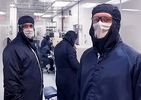
Turning revolutionary ideas into unique devices takes a talented, creative team:

  • Design engineers who translate brainstorms into brilliant circuitry
  • Skilled technical experts for layout, P&R, meticulous simulation, and deep verification
  • Hardcore logic gurus to craft embedded software
  • Process wizards who transform the design into exquisite, flawless silicon

We are that team.

First we pioneered 3DICs, then we developed proficiency in 2.5D, silicon interposers, chiplets, additive semiconductor manufacturing, and more.

Now our U.S.-based facilities provide end-to-end support, from design through packaging and test.

Together, we can create the future. 
https://nhanced-semi.com/wp-content/uploads/2024/04/About-1.png

ABOUT USA Firm Foundation

Turning revolutionary ideas into unique devices takes a talented, creative team:

  • Design engineers who translate brainstorms into brilliant circuitry
  • Skilled technical experts for layout, P&R, meticulous simulation, and deep verification
  • Hardcore logic gurus to craft embedded software
  • Process wizards who transform the design into exquisite, flawless silicon

We are that team.

First we pioneered 3D ICs, then we developed proficiency in 2.5D, silicon interposers, chiplets, additive semiconductor manufacturing, and more.

Now our U.S.-based facilities provide end-to-end support, from design through packaging and test.

Together, we can create the future. 

NEWS & RESOURCES

3DICs: The Least-Cost Option?
May 5, 2024
3DICs: The Least-Cost Option?
True 3DICs demonstrate prodigious improvement in performance and awesome savings in footprint and power, but they are commonly considered too expensive for widespread adoption. Not so, says Brian Bailey of Semiconductor Engineering: https://semiengineering.com/3d-ics-may-be-the-least-cost-option
Foundry 2.0™ Aims to Extend Moore’s Law
May 3, 2024
Foundry 2.0™ Aims to Extend Moore’s Law
Our revolutionary manufacturing model, Foundry 2.0™, allows us to tailor processes toward customized builds instead of mass production — a faster and less expensive way to extend Moore’s Law. Our President describes it in a blog post on 3D InCites: https://www.3dincites.com/2024/01/will-a-new-advanced-packaging-foundry-model-extend-moores-law
Purdue’s Atalla ASIP Institute
April 29, 2024
Purdue’s Atalla ASIP Institute
As Purdue’s neighbor at WestGate@Crane, we eagerly welcome the new Atalla Institute for Advanced System Integration and Packaging (ASIP). We look forward to exploring joint innovations with them and continuing to further next-gen tech in Indiana. https://purdue.edu/newsroom/releases/2023/Q4/purdues-new-institute-for-advanced-system-integration-and-packaging-honors-boilermaker-and-innovative-visionary-in-semiconductors.html
Need more information? Contact us any time.
https://nhanced-semi.com/wp-content/uploads/2024/01/NHanced-Logo-REV-RGB-WEB.png

Phone: +1 331-701-7070
Fax: +1 331-701-7055

© 2024 NHanced Semiconductors. All rights reserved.